Advancing Cu-Cu Hybrid Bonding: Overcoming Challenges for the Future of Semiconductor Packaging | Microwave Journal
Advancing Cu-Cu Hybrid Bonding: Overcoming Challenges for the Future of Semiconductor Packaging | Microwave Journal
IDTechEx released the Advanced Semiconductor Packaging 2023-2033 and Materials and Processing for Advanced Semiconductor Packaging 2024-2034, reports. encapsulating their in-depth analysis and insights into the rapidly evolving landscape of 3D semiconductor packaging.
As solder bump pitches shrink, several issues arise. Reduced bump height and surface area for bonding make it increasingly difficult to establish reliable electrical connections, necessitating precise manufacturing processes to avoid errors. Critical co-planarity and surface roughness become paramount, as even minor irregularities can compromise successful bonding.
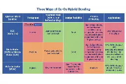
To overcome these issues, Cu-Cu hybrid bonding technology steps in as a game-changer. This innovative technique involves embedding metal contacts between dielectric materials and using heat treatment for solid-state diffusion of copper atoms, thereby eliminating the bridging problem associated with soldering.
The advantages of hybrid bonding over flip-chip soldering are obvious. Firstly, it enables ultra-fine pitch and small contact sizes, facilitating high I/O counts. This is critical in modern semiconductor packaging, where devices require a growing number of connections to meet performance demands. Secondly, unlike flip-chip soldering, which often relies on underfill materials, Cu-Cu hybrid bonding eliminates the need for underfill, reducing parasitic capacitance, resistance and inductance, as well as thermal resistance. Lastly, the reduced thickness of the bonded connections in Cu-Cu hybrid bonding, nearly eliminating the 10 to 30 micron thickness of solder balls in flip-chip technology, opens up new possibilities for more compact and efficient semiconductor packages.
Probably also makes for faster assembly times